about us
Professional PCB & PCBA production
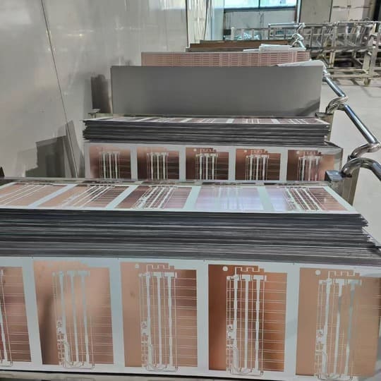
As a specialized LED PCB manufacturer, we deliver high-performance, energy-efficient circuit boards designed for superior brightness and durability. Whether for lighting, displays, or automotive applications, our precision-engineered LED PCBs ensure optimal thermal management and long-lasting performance.
Our advantages
Why Partner With Us?
✔ Thermal Excellence: Optimized metal-core designs for maximum heat dissipation.
✔ Precision & Quality: ISO-certified production with strict reliability testing.
✔ Custom Solutions: Tailored substrates for high-power LED, automotive, and industrial applications.
✔ Fast-Track Innovation: R&D support for next-gen lighting and electronic systems.
Driving Bright Ideas with Smarter PCBs – Your trusted partner for high-performance metal-core circuit boards.
Sample:24hours. And Mass production: 7 days
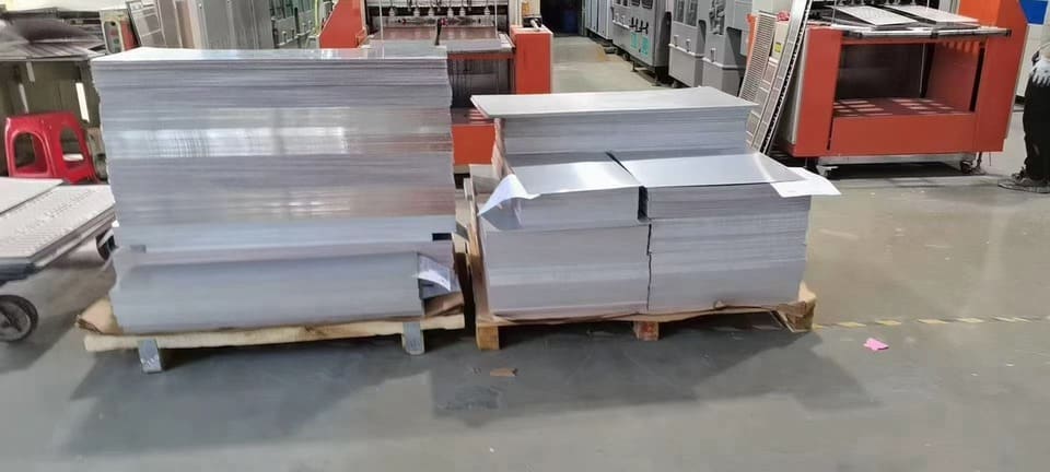
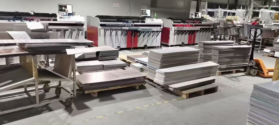
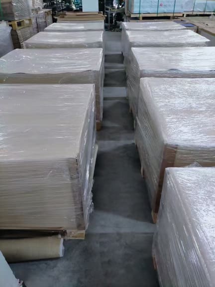
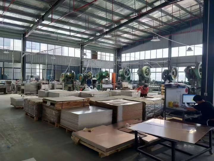
More than 100,000m² per month
Tailored substrates for high-power LED, automotive, and industrial applications.
ISO, ROSH, UL, SGS, IPC certified production with strict reliability testing.
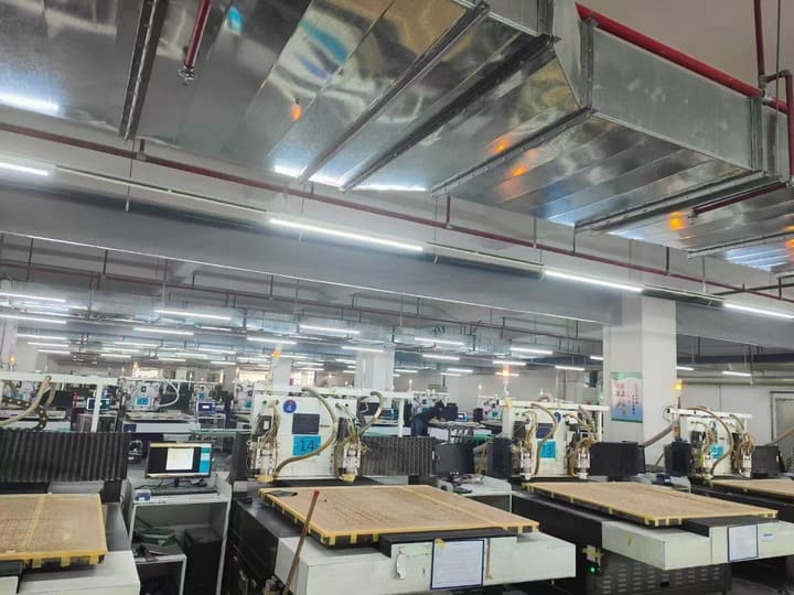
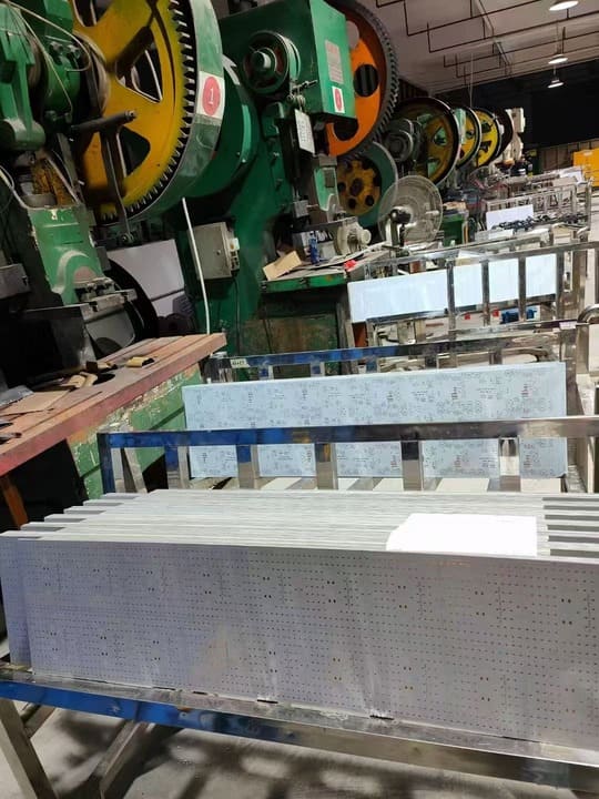
PCB production process
Engineered for Excellence, Built for Performance
Your Vision, Our Circuit – Superior PCBs Made Simple
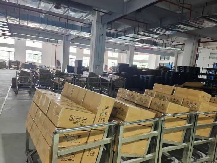
| Step | Process Stage | Description |
|---|---|---|
| 1 | Design and Output | Create PCB layout using EDA software and generate Gerber files |
| 2 | Print the Design | Print the circuit pattern onto a film |
| 3 | Inner Layer Imaging | Transfer the circuit image onto the inner copper layers using photoresist |
| 4 | Inner Layer Etching | Etch away excess copper, leaving behind the circuit pattern |
| 5 | Inner Layer AOI Inspection | Use Automated Optical Inspection to check for defects |
| 6 | Layer Lamination | Press all layers together to form a multilayer board |
| 7 | Drilling | Drill holes for vias, through-holes, and mounting |
| 8 | Plating (Electroless Copper) | Deposit a thin layer of copper inside the holes |
| 9 | Outer Layer Imaging | Transfer circuit image onto outer layers |
| 10 | Outer Layer Etching | Remove unwanted copper on outer layers |
| 11 | Outer Layer AOI Inspection | Inspect outer layers for accuracy and defects |
| 12 | Solder Mask Application | Apply solder mask to protect circuits and prevent short circuits |
| 13 | Surface Finish (e.g., HASL, ENIG) | Apply surface treatment to enhance solderability |
| 14 | Silkscreen Printing | Print labels, logos, and part identifiers on the PCB surface |
| 15 | Routing / V-Scoring | Cut the board into individual units or add break lines |
| 16 | Final Inspection & Electrical Test | Perform visual and electrical testing to ensure functionality |
| 17 | Packaging and Shipping | Pack finished boards and prepare for delivery |
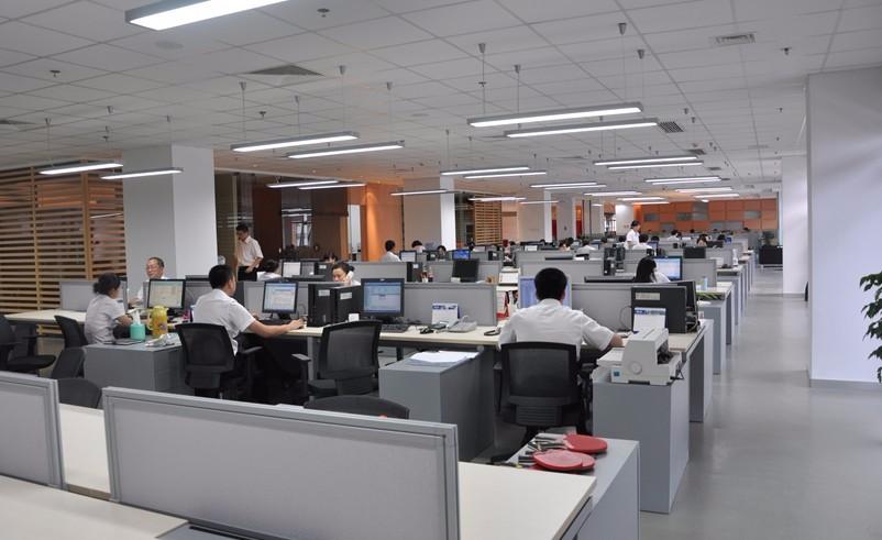
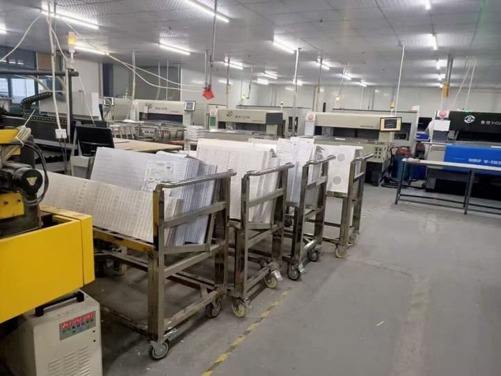
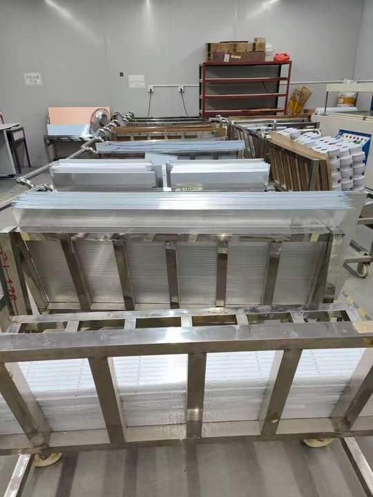
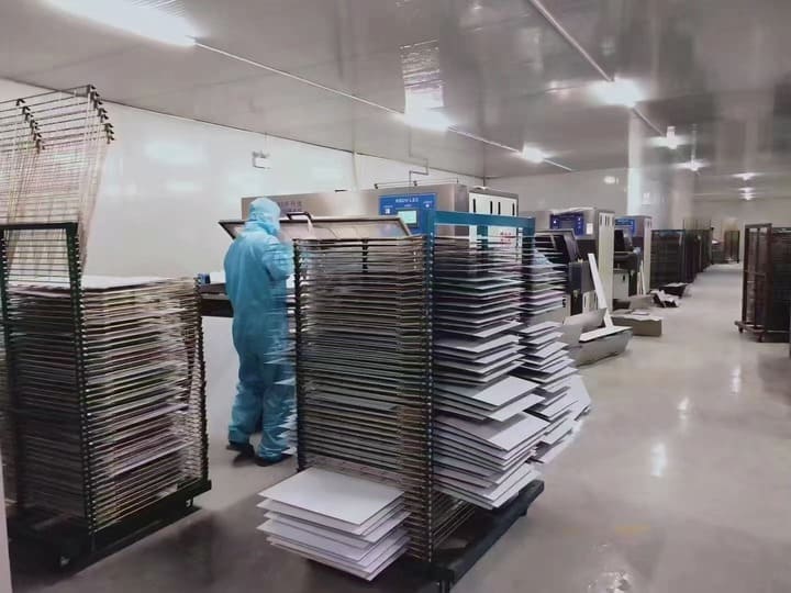
Our Factory
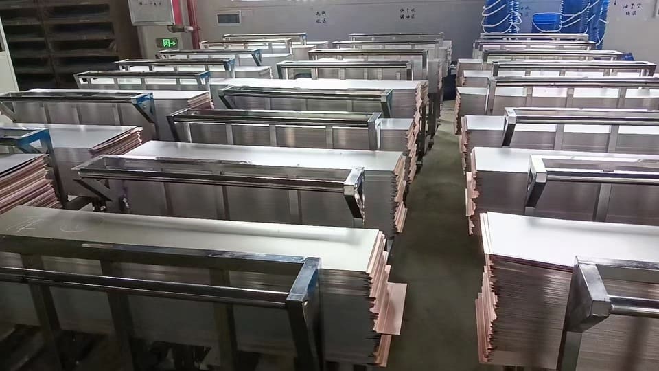
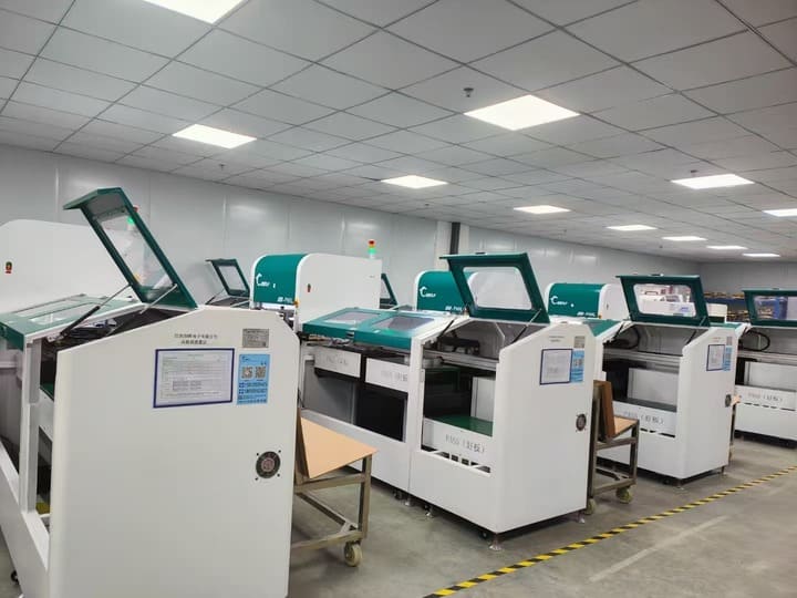
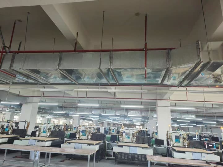
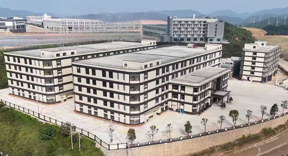

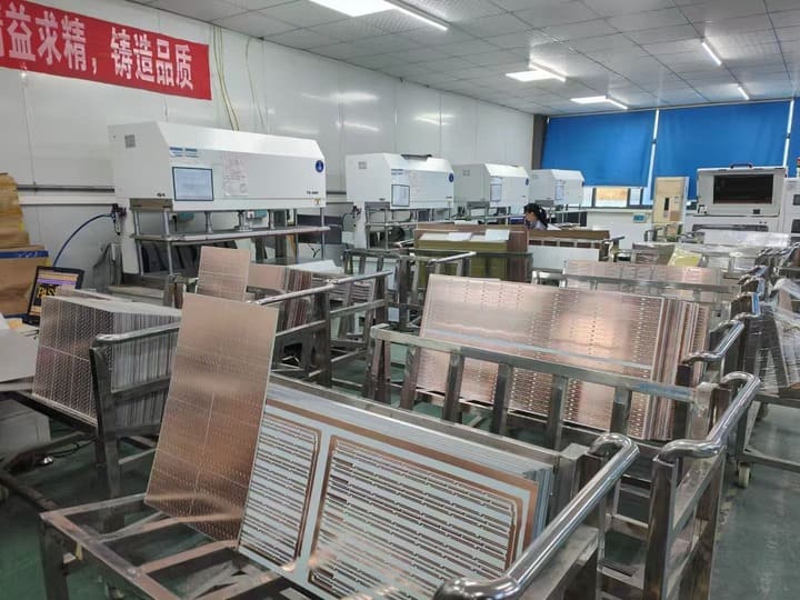
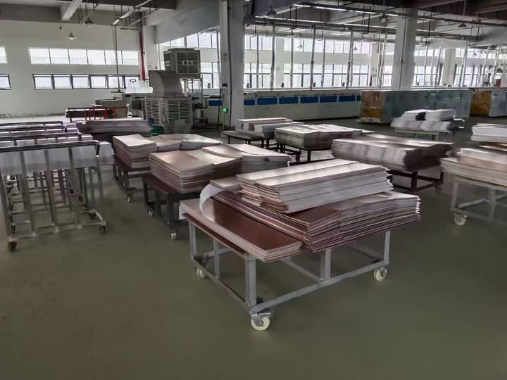
Experience
Expert LED PCB Manufacturing – Brighten Your Innovations
Our automated lines have increased production capacity by 30% while maintaining precision.